(China (Mainland))

Product Summary
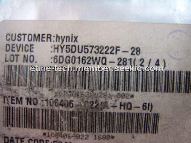
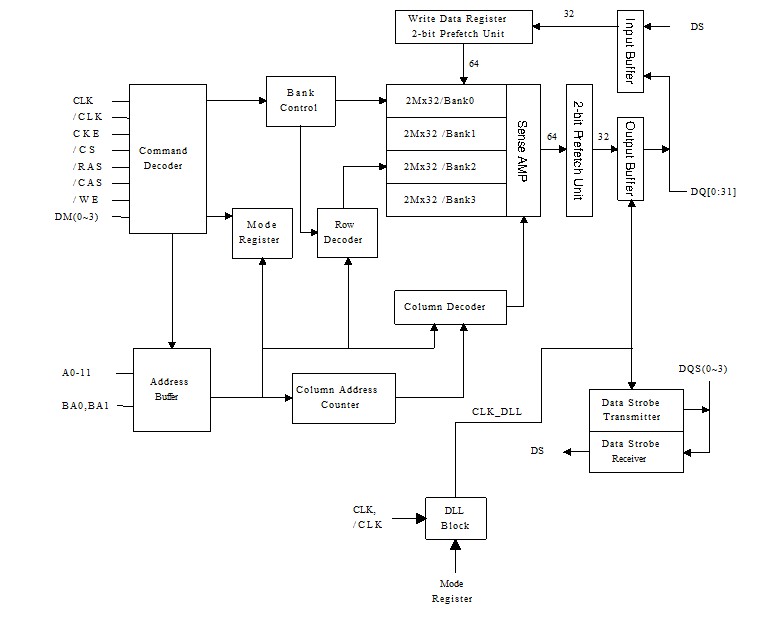
The HY5DU573222F-28 is a 268,435,456-bit CMOS Double Data Rate(DDR) Synchronous DRAM, ideally suited forthe point-to-point applications which requires high bandwidth. The HY5DU573222F-28 offers fully synchronous operations referenced to both rising and falling edges of the clock. While all addresses and control inputs are latched on the rising edges of the CK (falling edges of the /CK), Data, Data strobes and Write data masks inputs are sampled on both rising and falling edges of it.
Parametrics
HY5DU573222F-28 absolute maximum ratings: (1)Ambient TemperatureTA: 0 ~ 70°C; (2)Storage TemperatureTSTG: -55 ~ 125°C; (3)Voltage on Any Pin relative to VSSVIN, VOUT: -0.5 ~ 3.6V; (4)Voltage on VDD relative to VSS: -0.5 ~ 3.6V; (5)Voltage on VDDQ relative to VSS: -0.5 ~ 3.6V; (6)Output Short Circuit Current: 50mA; (7)Power Dissipation: PD: 2W; (8)Soldering Temperature·Time: TSOLDER: 260·10 °C·sec.
Features
HY5DU573222F-28 features: (1)The Hynix HY5DU573222F(P) guarantee until ; (2)200MHz speed at DLL_off condition; (3)2.5V VDD and VDDQ wide range max power supply supports; (4)All inputs and outputs are compatible with SSTL_2 interface; (5)12mm x 12mm, 144ball FBGA with 0.8mm pin pitch; (6)Fully differential clock inputs (CK, /CK) operation; (7)Double data rate interface; (8)Source synchronous - data transaction aligned to bidirectional data strobe (DQS0 ~ DQS3) ; (9)Data outputs on DQS edges when read (edged DQ) Data inputs on DQS centers when write (centered DQ); (10)Data(DQ) and Write masks(DM) latched on the both rising and falling edges of the data strobe; (11)All addresses and control inputs except Data, Data strobes and Data masks latched on the rising edges of the clock; (12)Write mask byte controls by DM (DM0 ~ DM3); (13)Programmable /CAS Latency 5 / 4 / 3 supported; (14)Programmable Burst Length 2 / 4 / 8 with both sequential and interleave mode; (15)Internal 4 bank operations with single pulsed /RAS; (16)tRAS Lock-Out function supported; (17)Auto refresh and self refresh supported; (18)4096 refresh cycles / 32ms; (19)Half strength and Matched Impedance driver option.
Diagrams
 |
 HY5DS113222FM |
Other |
|
Data Sheet |
Negotiable |
|
||||
|
HY5DS283222BF |
Other |
|
Data Sheet |
Negotiable |
|
||||
|
HY5DS283222BFP |
Other |
|
Data Sheet |
Negotiable |
|
||||
|
HY5DS573222F |
Other |
|
Data Sheet |
Negotiable |
|
||||
|
HY5DS573222P |
Other |
|
Data Sheet |
Negotiable |
|
||||
|
HY5DU121622A |
Other |
|
Data Sheet |
Negotiable |
|
||||